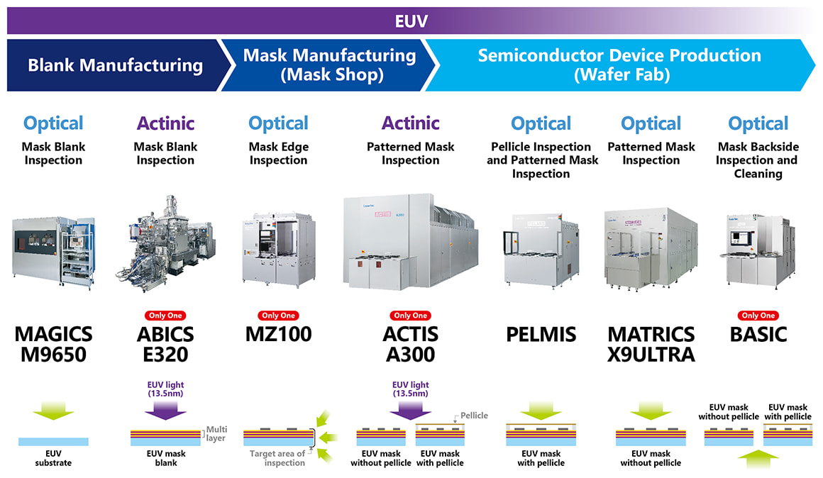
EUV Mask-related Inspection Systems
We embarked on the development of high-performance inspection systems for EUV lithography early on and have diligently devoted time and effort to acquire technical expertise in the area of EUV mask inspection. We have 6 products in our lineup today to meet customer needs.
Leading-edge semiconductor devices and EUV
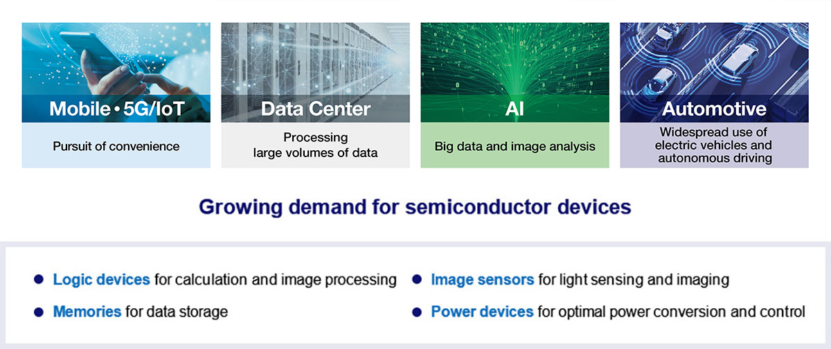
Semiconductor devices need to introduce finer and more complex IC designs to enjoy the merit of scaling and achieve better performance. Major device manufacturers have started using EUV lithography in volume production to print finer patterns on semiconductor chips since 2019. EUV lithography is a critical technology for manufacturing leading-edge semiconductors to enable the 5th generation mobile communication (5G), artificial intelligence (AI) and other innovations. The application of EUV lithography to semiconductor production is expected to grow rapidly.
As semiconductor devices attain a higher level of scaling and performance, inspection with better tools will be required.
As semiconductor devices attain a higher level of scaling and performance, inspection with better tools will be required.
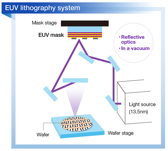
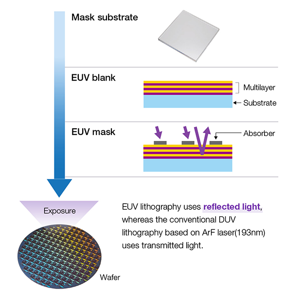
What is EUV lithography?
EUV lithography is a type of lithography using the extreme ultraviolet (EUV) range of light. It is capable of creating much finer IC patterns than previously possible because its wavelength (13.5nm) is much shorter than that of the ArF excimer laser (193nm) used in conventional DUV lithography.
- *Lithography is a technique to form patterns (e.g., line and space) on silicon wafers, which are eventually diced to make semiconductor chips. In lithography, wafers are exposed to light projected via a photomask, which is a plate with the blueprint of a pattern, after a photosensitive chemical called photoresist is applied on them. The pattern appears on the exposed wafers when the photoresist is removed from them. Multiple photomasks with different patterns are used to form an integrated circuit.
Lineup of EUV-related systems from Lasertec
Lasertec is offering solutions to the customer’s challenges by providing advanced inspection and measurement systems based on applied optical technologies, thereby contributing to society.
Lasertec is offering solutions to the customer’s challenges by providing advanced inspection and measurement systems based on applied optical technologies, thereby contributing to society.