Wafer Bump Inspection and Measurement System
BIM300
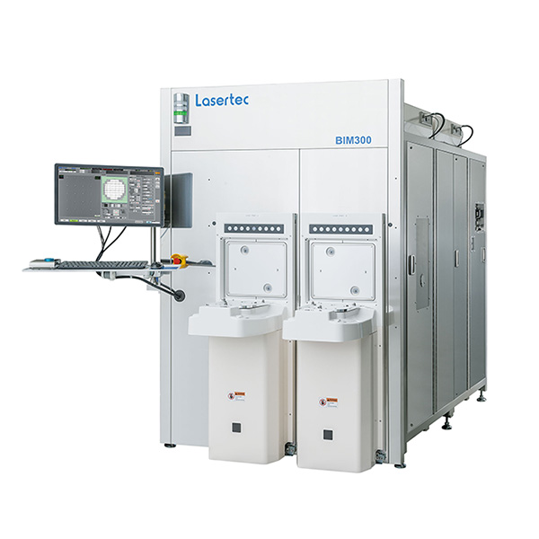
For accurate 3D measurement of bump shapes and wafer periphery quality control
Topics
Features
- Accurate measurement of height, width and shape based on confocal optics
- Automated in-line 3D measurement
- High resolution observation in a wide FOV that is not available with CD-SEM
Applications
- Measurement and inspection of bump's height, width and shapes in TSV process
- Observation and inspection of the peripheries of ground wafers for bonding, grinding process optimization and management
- Observation and measurement of particles, grinding traces and others on wafer surface
Specifications
| Dimensions (approximate) | 1,450mm (width) x 2,800mm (depth) x 2,100mm (height) |
|---|---|
| Applicable wafer size | up to 300mm |