Business and Core Technology
Business of Lasertec
Lasertec specializes in providing inspection and measurement solutions based on applied optics for semiconductor, FPD, and other industries.
Semiconductor-related products
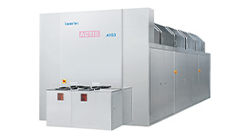
Inspection and measurement systems for mask blanks, photomasks and wafers
Our inspection and measurement systems play a crucial role in the semiconductor manufacturing process where the miniaturization of IC design continues to be made with the introduction of EUV lithography to volume production and the adoption of new materials and structures. In the segment of photomask-related inspection systems, our EUV mask blank inspection system has become a de facto standard tool, and our mask inspection systems have captured a large market share in the leading-edge lithography. In the segment of wafer-related inspection and measurement systems, we offer various solutions including those enabling wafer-edge inspection, whole-wafer film-thickness inspection, silicon thickness measurement, and SiC wafer inspection to meet customer needs.
Flat panel display (FPD)-related products
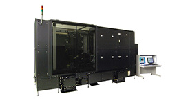
FPD photomask inspection systems
Our inspection systems for high-definition FPD photomasks have attained the status of a de facto standard tool in the industry.
Laser microscopes
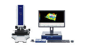
Hybrid laser microscopes offering both high performance and multi-functionality
Our laser microscopes are widely used among various industry customers engaged in R&D and quality control in such areas as semiconductor materials, transparent films, coating materials, inorganic/organic materials, biological samples, metal parts, and plastic components.
Core Technology
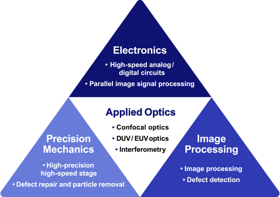
The core technology that enables Lasertec to create epoch-making products is applied optics.
Lasertec has accumulated its own proprietary technologies by pursuing the ultimate possibility in the use of light for inspection and measurement. It began with our success in developing a "laser microscope" through the effort to use a laser light source to achieve high resolution. Since then, we have mastered a "confocal optics" technology that enables the construction of all-in-focus, three-dimensional images of samples. We have also succeeded in developing a "DUV/EUV optics" technology that addresses the need to use a shorter wavelength light source in semiconductor lithography that has emerged with scaling, and an "interferometry" technology that accurately measures very small shifts in the phase of light.
We combine these core technologies in applied optics with other technologies in peripheral areas to offer the best solution to each application. We meet various customer needs in this manner.
History of Lasertec, origin of company name, the world's first products from Lasertec.