More Information


Corporate strategy
We provide solutions that address customer needs quickly. We keep a flat and flexible organization to enable quick decision-making, quick action for customers, and rapid product development.
We strive to achieve high market shares and high profit margins in market segments where we can offer differentiated solutions to meet the demanding requirements of customers for technology level and value-added solutions. We stay in close contact with global leading companies in the semiconductor industry and establish a solid relationship built on trust.
We outsource production to subcontractors, and this allows us to have a lot of freedom in business execution. We concentrate the allocation of resources on R&D (with roughly 70% engineer ratio and 5% - 10% R&D ratio) to keep developing new products.
Our global position
Lasertec's position
Market
Semiconductors are expanding their applications into various fields, such as AI, IoT, 5G, and data centers, and contributing to making a better, more affluent society. They keep evolving and achieving higher performance with the pursuit of smaller geometries as well as through the development of new structures and new materials. There are many steps in semiconductor manufacturing process, and various manufacturing tools are required to complete all the steps. Among such tools, Lasertec specializes in inspection and measurement systems that utilize applied optical technology and provides solutions that perfectly fit customer needs.
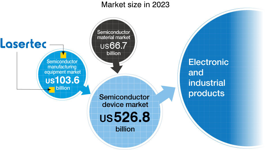
Illustration by Lasertec based on WSTS semiconductor market forecast spring 2025 and SEMI semiconductor equipment sales forecast in July 2025
Illustration by Lasertec based on WSTS semiconductor market forecast spring 2025 and SEMI semiconductor equipment sales forecast in July 2025
High global market share
Our inspection and measurement systems play a crucial role in semiconductor manufacturing process where performance improvements are required all the time. As a leading supplier of semiconductor mask and mask blank inspection systems, we provide one-of-a-kind systems in the world and systems that have a high market share in the global market.
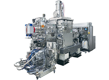
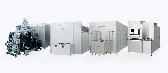
EUV Mask Blanks Inspection and Review System
ABICS Series E320
Actinic EUV Patterned Mask Inspection System
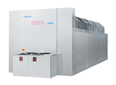
ACTIS A300 Series
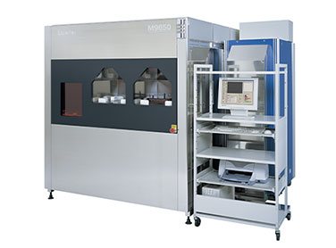
Mask Blanks Inspection and Review System
MAGICS Series
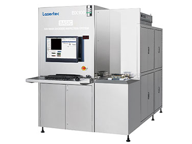
EUV Mask Backside Inspection and Cleaning System
BASIC Series
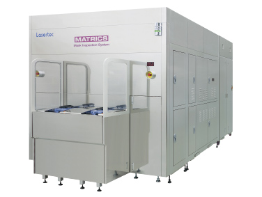
Mask Inspection System
MATRICS X9ULTRA Series
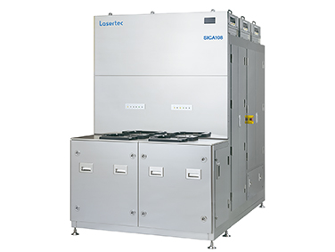
SiC Wafer Inspection and Review System
SICA108
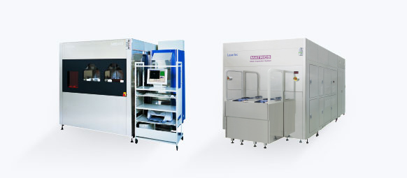
Business areas
Inspection and measurement systems for mask blanks, photomasks, and wafers
Inspection systems for FPD photomasks
High-performance, multi-functional hybrid laser microscopes
Products in focus
EUV mask-related inspection systems
Lasertec embarked on the development of high-performance inspection systems for EUV lithography early on and has diligently devoted time and effort to acquire technical expertise in the area of EUV mask blank inspection and EUV mask inspection. Click below to see our mainstream EUV-related products.
Semiconductor-related inspection systems
Semiconductor devices are manufactured by printing very small integrated circuits (ICs) on silicon wafers by transferring IC patterns from their blueprints on photomasks in a process called lithography. Photomasks must be flawless, and Lasertec's inspection systems are used to inspect these photomasks and their unpatterned plates with optical technology. Click below to see our products for conventional lithography.