Lasertec launches a new wafer edge inspection system, EZ300
2015.11.26
For wafer edge yield management and process error analysis
Lasertec Corporation announced today that it has launched EZ300, a wafer edge inspection system of new concept that contributes to higher yields at wafer edges in the production of semiconductor chips. Lasertec will introduce the new product at SEMICON Japan 2015 in Tokyo Big Sight on December 16 to 18 and illustrate how the new tool can be utilized effectively.
Description
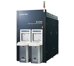
EZ300 uses confocal optics, a core technology of Lasertec, for inspection, review and measurement of wafer edges and embodies "All in One Concept" covering the entire in-line inspection needs up to root cause analysis for each defect type within a single platform.
Until today, it was considered a tough challenge to detect and identify defects of interest (DOI) at wafer edges in production lines. EZ300 offers a solution to the challenge with a combination of its high-resolution confocal optics and proprietary software algorithm, making it possible to perform automatic defect classification, including pit/bump analysis, and size measurement during inspection. This will enable users to establish in-line QC based on statistical process control (SPC) and to track down the cause of chip defects.
Hitherto-available wafer edge inspection tools require the use of SEM or AFM for defect classification and measurement. The conventional method is time-consuming and costly because defect position matching for multiple tools takes a long time. In contrast, EZ300 single-handedly offers 3D measurement of defects - width, height and roughness - based on its high-resolution reviews as well as defect classification based on image processing, thereby helping users achieve quick process feedback and optimization.
The scaling of integrated circuits has brought a reduction in power consumption and an increase in the number of transistors printed on a chip, achieving higher performance and lower cost. However, further scaling is facing various technical difficulties such as leak electricity. To meet the challenge, manufacturers have introduced new device structures that entail higher complexities in film layers. However, this has led to a problem of lower production yields at wafer edges due to undesirable particle generation. Besides, the industry is trying to expand the usable area of wafer in order to increase overall productivity. For this reason, it is now considered more important to take on yield management at wafer edges. Furthermore, the introduction of 3D IC using through silicon via (TSV) and 3D memory chips with vertically formed transistors has brought new processes that make the quantitative management of wafer edges even more important.
EZ300 is a system that performs inspection, review and measurement altogether to address such customer needs. It is a versatile tool that meets the requirements of in-line quantitative management and process development analysis. Lasertec will continue its effort to facilitate yield improvement and higher productivity using its core technologies and contribute to the further progress of the semiconductor industry.
Key Features
- Defect inspection using high contrast images from confocal optics
- Automatic defect classification including pit/bump analysis by proprietary algorithm
- High-resolution 3D measurement that facilitates defect type identification and estimation
Applications
- Quantitative management of wafer edges for in-line QC and early warning of process errors
- Follow-on analysis of chip defects at wafer edges using SPC
- Root cause analysis of yield loss at wafer edges