Lasertec releases new EUV Mask Blank Inspection and Review System ABICS E120
2017.04.03
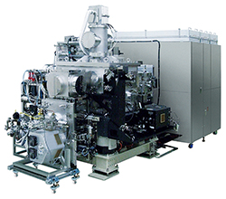
Detecting printable phase defects and enabling defect management for EUV mask blanks
Lasertec Corporation has released ABICS E120, a EUV mask blank inspection and review system that contributes to defect management and yield improvement in the production of EUV mask blanks. The new system will be introduced at Photomask Japan 2017, which begins on April 5, 2017.
Description
Lasertec has been engaged in advanced technology development in the field of photomask and mask blank inspection for many years. Technologies gained through this effort have produced high-sensitivity mask blank inspection systems used in outgoing mask blank inspection and process control. These systems have earned a high reputation in the industry.
The progress in the scaling of semiconductor devices has now reached a point where the extreme ultraviolet (EUV) light, long regarded as the exposure light of the next-generation semiconductor lithography, is about to be used for commercial application. There arises an imminent need for having an inspection system that enables the quality control of EUV mask blanks.
Lasertec participated in a joint R&D program of EIDEC1 for 5 years from 2011 to develop a EUV mask blank inspection system named Actinic Blank Inspection (ABI) 2 under the sponsorship of New Energy and Industrial Technology Development Organization, a governmental organization of Japan.
In this background, Lasertec has launched ABICS E120, a new EUV mask blank inspection and review system designed to meet the needs of semiconductor production with EUV lithography, based on the technologies accumulated through the joint development of ABI.
The use of EUV light for inspection and review enables ABICS E120 to selectively detect printable defects and to perform defect analysis with the EUV light. ABICS E120 will make a significant contribution to defect management and yield improvement in the production of EUV mask blanks.
- *1EIDEC is a Japan-based international consortium. At the time of joint development program, EIDEC was known as EUVL Infrastructure Development Center. Its current name is Evolving Nano-process Development Center.
- *2ABI uses the same wavelength of exposure light used for EUV lithography.
Features
- Actinic inspection (with the 13.5nm EUV light)
- High-sensitivity detection of printable phase defects inside Mo/Si multilayer
- High-sensitivity and high-speed inspection with dark-field optics
- Highly accurate capturing of defect coordinates with high magnification review
- Defect analysis with bright-field and dark-field reviews
Applications
- EUV mask blank (Mo/Si multilayer) inspection
- EUV mask blank defect analysis
- High-accuracy defect location detection