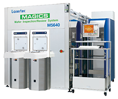
Wafer Inspection / Review System M5640
2008.11.14
High sensitivity defect inspection/review system, implementing minute defect detection required by the next generation processes
Lasertec releases a newest model, Wafer Inspection/Review System [M5640], which implements both high throughput and high sensitivity.
Description
Lasertec's product series MAGICS has established its position as a de facto standard in the industry, because this product series is widely used for evaluation and analysis of wafer and also for process improvement. MAGICS series products provide the following features based on confocal optics that is the core technology of Lasertec. These features are not implemented by the light-scattering-based inspection systems.
- High detection capability of killer defects such as PID, Shallow scratch, COP, SF and the like, which originate to the process itself.
- Defect class verification by high-speed and high-resolution review
- High sensitivity inspection of epitaxial wafer, quartz wafer and such, which is difficult for light scattering methods to achieve due to influences of haze and back surface reflection
Demand for higher quality wafers of various kinds is intensifying and subsequently, requirements for inspection tools are becoming more demanding, due to pursuit of ever finer design rule. Consequently, the need to reduce the number of defects that are difficult to detect by the light scattering type inspection system, is intensifying.
M5460 has implemented high detection sensitivity and reduction of inspection time by half while maintaining the performance characteristics of the conventional MAGICS products. Furthermore, the back-surface non-contact chucking is selectable, which makes this system applicable to outgoing and incoming inspections, in addition to process evaluation and process analysis.
Key Features
- Further improved sensitivity for killer defects such as PID, Shallow scratch, COP, SF and so on that are generated in wafer manufacturing processes.
- Quick defect class verification by high-speed and high-resolution review function based on confocal optics supports speedy improvement of wafer quality.
- High precision defect coordinate verification and dust-free defect position marking with a diamond chip make the process monitoring, such as analysis of root cause for defect generation, easy. Verified defect coordinates greatly contribute to further analyses by SEM, TEM, AFM and so on.
- Besides mirror polish wafer, wafers covered by layers such as epitaxial wafers and SOI wafers that are vulnerable to haze, can be inspected with high sensitivity.
- Quartz wafer, difficult to be inspected by the light scattering method due to the effect of scattered light from wafer back surface and wafer chucking mechanism, can be inspected by similar sensitivity as that for wafers covered by layers.
- Introduction of newly developed 63 multi beam optics and stage of light weight with low gravity point implements throughput twice as high.Power saving function and longer lifetime of the laser light source reduces CoO by 40%.
- Wafer handling can be selected from two kinds of specifications.
- Outgoing and incoming inspection: Edge-grip and back surface non-contact chuck
- Evaluation and analysis: Vacuum suction chuck for multi-sizes (6, 8 and 12 inches)
- Compatible with FOUP and FOSB open cassettes
Applications
- Evaluation and improvement of wafer manufacturing processes
- Outgoing and incoming inspections of wafers
- Development of materials for polishing and cleaning