New Product: "GALOIS" Series GaN Wafer Inspection and Review System
2017.12.04
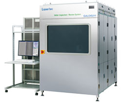
Detecting various GaN wafer defects faster and enabling high-resolution defect observation
Lasertec Corporation today announced the launch of a new defect inspection and review system series named "GALOIS", which is designed specifically for the inspection and analysis of gallium nitride (GaN) wafers. They are already accepting orders.
Description
The GALOIS Series uses bright-field confocal optics, enabling high-speed inspection of various kinds of GaN wafer defects and high-resolution observation of defect images.
Amid increased awareness of energy saving on a global scale, there is growing demand for new technologies that achieve energy efficiency at an extremely high level. Silicon carbide (SiC) and gallium nitride (GaN) are materials that have high potential to make this possible. There is intensive R&D aimed at improving the quality of wide-bandgap semiconductors using these materials and lowering their cost, making them suitable for commercial use in applications such as power electronics, high-speed communication, and LEDs.
SiC is already moving ahead in commercial applications. Lasertec's SICA88 is widely used as the de facto standard SiC inspection tool, enjoying strong market recognition due to its high throughput, high accuracy of defect classification, high-resolution defect review, and more.
GaN, on the other hand, lags behind in device usage, hindered by the high cost of GaN wafer manufacturing and the presence of numerous crystallographic and process defects in wafers, requiring further efforts in wafer quality improvement. The Lasertec GALOIS Series, which offers the high-speed, high-sensitivity detection and classification of crystallographic and process defects, combined with high-resolution defect image review, has been launched to assist these efforts.
GALOIS uses a combination of confocal optics and differential interferometry optics - both of which are Lasertec core technologies - with a sophisticated algorithm based on advanced imaging technology. This eliminates the effect of noise from the backside of a transparent substrate, or from surface morphology, enabling the high-sensitivity detection of various kinds of defects in GaN wafers.
GALOIS employs a high-speed processing computer system and a model based on machine learning, including advanced Deep Learning, for defect classification. GALOIS uses the high-resolution review images captured by the above mentioned Lasertec core technologies and accurately classifies indeterminately formed defects, in parallel with other inspection processing.
All review images captured during inspection of whole wafers are saved to computer storage, and can be utilized for analysis of unclassified defects. GALOIS achieves an inspection speed of 6 minutes per 6-inch wafer, which is fast enough for future application in the production phase.
In addition to being an outgoing and incoming inspection tool for GaN wafers, GALOIS also takes the role of a strong process and yield improvement tool. It helps in identifying the root cause of defects, acting as a wafer, epitaxy, and device process monitor.
Lasertec will continuously endeavor to develop advanced inspection technologies and contribute to the yield improvement of next-generation devices.
Features
- Confocal optics - best suited for transparent wafer inspection - eliminates the effect of noise from the backside of the wafer
- Differential interferometry captures shallow-scratch and various crystallographic defects with high sensitivity
- Wavelength selection by light source and optical filters enables the inspection of wafers with GaN-on-SiC or other hetero-epi structures under optimal conditions, unaffected by thin-film interference
- Advanced image processing technology enables inspection which is unaffected by GaN surface morphology
- High-speed inspection at 6 minutes per 6-inch wafer extends use to the production phase
- Defect mapping, defect classification, and marking functions support defect analysis
Applications
- Bulk GaN wafer inspection
- GaN epitaxial layer (homo-epi and hetero-epi) inspection
- Analysis of changes in defect characteristics before and after heat processing in the device making process
- Management of the epitaxy process and processing tools
- Management of grinding material development and grinding processes