GaN Wafer Inspection and Review System
GALOIS211
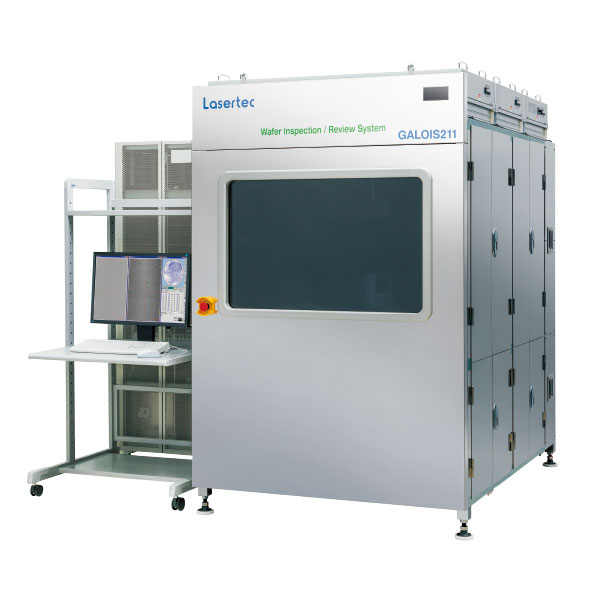
Detecting various GaN wafer defects faster and enabling high-resolution defect observation
Topics
Features
- Confocal optics - best suited for transparent wafer inspection - eliminates the effect of noise from the backside of the wafer
- Differential interferometry captures shallow-scratch and various crystallographic defects with high sensitivity
- Wavelength selection by light source and optical filters enables the inspection of wafers with GaN-on-SiC or other hetero-epi structures under optimal conditions, unaffected by thin-film interference
- Advanced image processing technology enables inspection which is unaffected by GaN surface morphology
- High-speed inspection at 6 minutes per 6-inch wafer extends use to the production phase
- Defect mapping, defect classification, and marking functions support defect analysis
Applications
- Bulk GaN wafer inspection
- GaN epitaxial layer (homo-epi and hetero-epi) inspection
- Analysis of changes in defect characteristics before and after heat processing in the device making process
- Management of the epitaxy process and processing tools
- Management of grinding material development and grinding processes
Specifications
| Dimensions | 3,052mm (D) x 3,250mm (W) x 1.990mm (H) ※Including maintenance space |
|---|---|
| Wafer size | Up to φ8 inches |
| Applicable wafer types | Bulk GaN, homo-epi and hetero-epi GaN wafers |
| Inspection time | 6 minutes per wafer (φ6 inch wafer, with 10x lens) |