High Sensitivity Wafer Edge Inspection System
CIEL Series
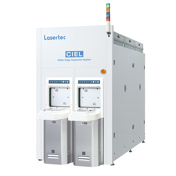
Highly accurate classification of wafer edge and bevel defects that are not detectable by existing tools
Topics
Features
- Identification of small defects that cannot be detected or classified by existing tools
- A high-throughput mode adaptable to meet operational needs
- 3D profiling capability
Applications
- Wafer edge and bevel inspection for process monitoring and feedback in semiconductor device manufacturing processes
- Identification of yield-critical defects
- Process improvement based on 3D measurement
You might also be interested in