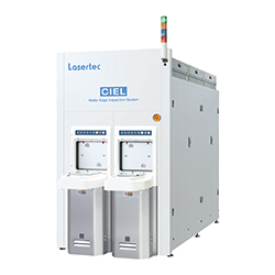
Lasertec releases CIEL Series High Sensitivity Wafer Edge Inspection System
2022.12.01
Highly accurate classification of wafer edge and bevel defects that are not detectable by existing tools
Lasertec announced the release of the CIEL series, a high sensitivity wafer edge inspection system.
Description
As the design of semiconductors becomes increasingly downsized and multilayered, chipmakers find smaller and more diverse defects originating from the wafer edge. This has led to a growing demand for a tool that can detect and identify only those defects that negatively affect yields in semiconductor production among a multitude of defects.
The CIEL series introduces newly designed proprietary optics, a complete makeover from EZ300’s, to achieve high-sensitivity, high-throughput inspection. It is designed to identify defects of interest accurately by using highly accurate defect classification based on deep learning and by capturing high-resolution images containing height/depth information with the 3D profiling function of our proprietary optics.
Lasertec will continue to support the needs of leading-edge semiconductor manufacturing processes and contribute to the efforts of quality and yield enhancement.
Key Features
- Identification of small defects that cannot be detected or classified by existing tools
- A high-throughput mode adaptable to meet operational needs
- 3D profiling capability
Applications
- Wafer edge and bevel inspection for process monitoring and feedback in semiconductor device manufacturing processes
- Identification of yield-critical defects
- Process improvement based on 3D measurement