Green Product Development Policy
- Our basic policy is to keep developing leading-edge inspection systems that facilitate the advancement of semiconductor scaling and that help customers achieve yield improvement in their manufacturing process, thereby lowering power consumption*1 and contributing to the lessening of environmental burdens*2.
- We take the efficiency of energy and resource use into consideration when engaging in product development, designing, manufacturing, and sales promotion, and promote the reduction and recycling of waste.
Lower power consumption achieved by semiconductor scaling
We are surrounded by many electronic products in our daily life, and semiconductor devices (integrated circuits) are playing a crucial role in making them work.
- Lower power consumption achieved by leading-edge semiconductor chips
- According to the scaling rule of semiconductors, with the shrinking of an integrated circuit to 1/k of its original scale, in theory, its functioning speed becomes proportionally faster to k times the original speed while both its area and power consumption become exponentially smaller to 1/k2 of their original figures. For example, if we shrink an integrated circuit to 1/2 of its original scale, its calculation speed will become twice as fast while its area and power consumption will become 1/4 of their original figures. The reason why the semiconductor industry is making all the effort of introducing EUV and other state-of-the-art technologies for the advancement of scaling is to enjoy this merit. Since there is a cancelling effect of increased leak current, we do not see 100% of the merit in the real world. However, IC chips still achieve a significant saving of power consumption per bit from the scaling. According to a publicly available statement by a major foundry, up to 30% power reduction is expected to be made by the next-generation leading-edge IC chips, compared with the previous generation chips.
Our inspection and measurement systems' contribution to the lessening of environmental burdens
- Leading-edge semiconductor
-
A mask (or photomask) is a glass plate with an integrated circuit pattern formed on its surface. It serves as a blueprint of the pattern to be copied onto wafers by a technique called lithography. Defects and particles on the photomask will also be copied onto wafers together with the IC pattern and if they are present, albeit tiny and few, the entire lot of wafers will become defective and have to be discarded.
Mask inspection systems and mask blank inspection systems are designed to detect extremely tiny defects and particles on the photomasks. They are crucial for the quality assurance of semiconductor IC chips and for reducing defective chips (i.e., improving production yields). In other words, our products contribute to the production of high-performance, highly energy-efficient semiconductor devices. They also contribute to reducing the waste of wafers and glass substrates and minimizing the consumption of chemical substances during production. This is how they contribute to the lessening of environmental burdens.
- Next-generation power semiconductor and other areas
- In addition to these mainstream products, we offer wafer inspection systems that facilitate the widespread use of next-generation power semiconductors made of silicon carbide (SiC) and gallium nitride (GaN), both of which are materials with excellent energy properties that enable the attainment of significantly higher power efficiency. We also offer a system that is being used as a tool to analyze the performance of high-end lithium ion batteries to develop better and safer batteries, which are necessary to make electric vehicles more reliable and affordable. We also have de facto standard inspection tools that contributed to the commercialization of FPDs such as LCD and OLED to replace CRTs, facilitating a significant reduction in the power consumption of displays.
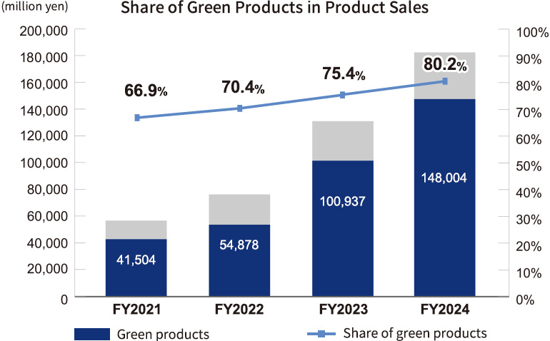
Our Green Products
We consider the following product groups as Green Products because they are particularly effective in helping semiconductor devices achieve lower power consumption and for the development of lithium-ion batteries:
・EUV mask-related equipment
・Power semiconductor-related equipment
・Lithium-ion battery-related equipment
| FY2021 | FY2022 | FY2023 | FY2024 | FY2025 | |
|---|---|---|---|---|---|
| Sales of Green Products | 41,504 | 54,878 | 100,937 | 148,004 | 156,999 |
| Ratio of Green Products in Total Product Sales | 66.9% | 70.4% | 75.4% | 80.2% | 75.3% |
R&D Investment in Green Products – Result and Target
Our R&D investment in the areas related to Green Products totaled about 28 billion yen during the five years from FY2019 to FY2023. We expect continued growth in those areas and therefore foresee a total R&D investment of 50 billion yen or more during the next five years (FY2024 to FY2028).
| FY2024 | FY2025 | |
|---|---|---|
| R&D Investment in Green Products | 11,252 | 9,816 |
Examples of Our Efforts to Develop Environmentally Friendly Products
- ACTIS
-
The ACTIS series is an actinic EUV patterned mask inspection system that uses EUV light, which has a much shorter wavelength than conventional DUV light, for the light source of inspection. It achieves a significant improvement in defect detection sensitivity and enables the detection of phase-shift defects unique to EUV masks. Used in the production process of leading-edge semiconductors, ACTIS is making a significant contribution to the improvement of semiconductor performance and energy efficiency, thereby helping the advancement of nanotechnology. Lasertec has developed URASHIMA, an in-house EUV plasma light source for ACTIS with an optimized design showing a notable improvement in environmental performance. ACTIS units equipped with URASHIMA have been delivered to customers for use in high-volume manufacturing. URASHIMA achieves a significant reduction in environmental impact, cutting the consumption of tin used to generate EUV light to 1/100 and power consumption to 1/3 compared to the previous EUV light source.
- SICA
-
The SICA series is a SiC wafer inspection and review system widely used in SiC wafer/device production processes and playing a significant role in making SiC power semiconductors more reliable and affordable. Silicon carbide or SiC is highly anticipated as a material for next-generation power semiconductors. It has superior properties, for example, 110 times the dielectric strength and 23 times the energy band gap compared to the conventional material, silicon or Si. SiC improves the durability of power semiconductor devices and reduces power loss. Because of these properties, SiC devices are becoming widely popular for use in various applications, including industrial equipment, electric vehicles, and solar/wind power plants. The SICA series is contributing to yield improvement and cost reduction in the high-volume manufacturing of SiC power semiconductors, facilitating the realization of a carbon-neutral society.
- GALOIS
-
The GALOIS series is a GaN wafer inspection and review system that detects defects in wafer production processes. It plays a significant role in making GaN-based power semiconductors more usable. GaN is a material with higher dielectric strength and stabler internal structure than SiC. Because of its high-frequency switching capability, GaN enables the use of high-frequency power supplies and helps shrink the size of device designs. The GALOIS series uses confocal optics and differential interferometry optics, both Lasertec’s core technologies, together with machine-learning algorithms, including deep learning, to enable the high-sensitivity detection and highly accurate classification of various indeterminately shaped defects.
- CIEL
-
The CIEL series is a high-sensitivity wafer edge inspection system that uses Lasertec’s proprietary optics and deep learning to enable the detection and classification of only those defects that impact semiconductor yields among a multitude of defects originating from the wafer edge. It helps semiconductor device manufacturers achieve quality enhancement and yield improvement.
- ECCS B320
-
The ECCS series contributes to quality enhancement and new material development for lithium-ion batteries by enabling the observation of electrochemical reactions that occur inside during charging and discharging with real-time color imaging.
- OPTELICS
-
The OPTELICS-series laser microscope offers an all-in-one solution for inspection and measurement of various materials, including different types of semiconductor wafers. It provides optimal solutions for R&D and mass production needs, facilitating a broad range of development efforts, and contributing to improved productivity. OPTELICS harnesses AI technology by using machine learning algorithms, including deep learning, to capture and classify diverse defect images. This helps widen its inspection applications greatly.
- Efforts to Reuse and Recycle
-
We refurbish and reuse laser light sources and lamp modules, key components of our products that require periodic replacement. If a component used in one of our products is discontinued, we strive to find an alternative component to extend service life as much as possible. We also use reusable packaging materials whenever possible.